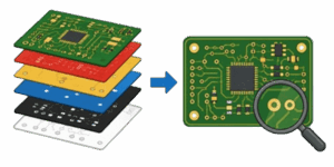
Sending 1 circuit board design to a fabrication house always feels like a leap of faith. You might spend 40 hours routing complex differential pairs, meticulously running your design rule checks, and balancing your layer stackup. Then you hit the export button, upload a zipped folder to a manufacturer halfway across the world, and wait 2 weeks for the physical boards to arrive. If you are lucky, the hardware works perfectly on the 1st revision. If you are not, you might find solid copper poured over your mounting holes or silkscreen text printed directly onto your surface mount pads.
✍ In the field, we often see junior engineers trust their software design rule checks blindly. The reality is that your computer aided design software does not manufacture the board. The fabrication house relies entirely on the exact exported output you provide. That output is almost universally formatted as Gerber data. Understanding how to read, interpret, and troubleshoot these files is the single most important skill a hardware designer can develop to prevent costly manufacturing failures.
Table of Contents
The Genesis of the RS-274X Standard
To understand the file format, you must understand the physical machinery it was designed to control. In the 1960s, Joseph Gerber invented the photoplotter. Before this invention, engineers created printed circuit boards using black tape on clear Mylar sheets, which were then photographically reduced. The photoplotter automated this by moving a directed beam of light across a large sheet of photographic film. The machine required a specific language of coordinates and commands to know where to open the mechanical shutter and where to move the light source.

That legacy lives on today. Modern circuit boards are manufactured using laser direct imaging, but the instruction set remains largely the same. When you generate a Gerber file, you are creating a 2D ASCII text file that acts as numeric control code for a light beam. The current global standard is RS-274X, which embeds all the necessary aperture definitions directly within the file, eliminating the need for a separate tool list.
The Physics of Photoplotting and Acid Etching
Every layer of your circuit board requires 1 dedicated Gerber file. The top copper, the bottom copper, the top solder mask, and the top silkscreen are all distinct files. During fabrication, a raw panel of fiberglass laminate clad with solid copper is coated in a light-sensitive photoresist. The manufacturer uses your copper Gerber file to expose this photoresist. The areas struck by ultraviolet light harden. The unexposed areas remain soft and are chemically washed away.
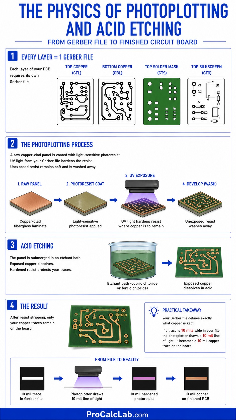
The panel is then submerged in an etchant bath, typically cupric chloride or ferric chloride. The hardened photoresist protects your traces, while the exposed copper dissolves into the acid. From a practical standpoint, this means your Gerber file must explicitly define the exact geometry of the copper you wish to keep. If a trace is 10 mils wide in your file, the photoplotter draws a 10 mil line of light, which eventually becomes a physical 10 mil copper wire.
Demystifying the Layer Stackup
📊 A standard 4-layer board requires a minimum of 10 distinct files to manufacture correctly. Identifying them by their file extensions is the 1st step in reading the data archive. Different software packages output different extensions, but the underlying ASCII data remains identical.
The top copper layer defines your component pads and top-level routing. The inner layers define your power planes and ground planes. The solder mask layers define the negative space where the green protective coating should be absent, allowing you to solder components. A common mistake during calculations is forgetting that the solder mask is a negative image. Drawing a shape on the solder mask layer means you are removing the mask in that specific area, not adding it.
The Mathematics of Trace Current Capacity
Before you even generate your manufacturing data, you must ensure your copper traces can physically carry the required electrical current without overheating and delaminating from the fiberglass substrate. The industry relies on the IPC-2221 standard for these calculations.
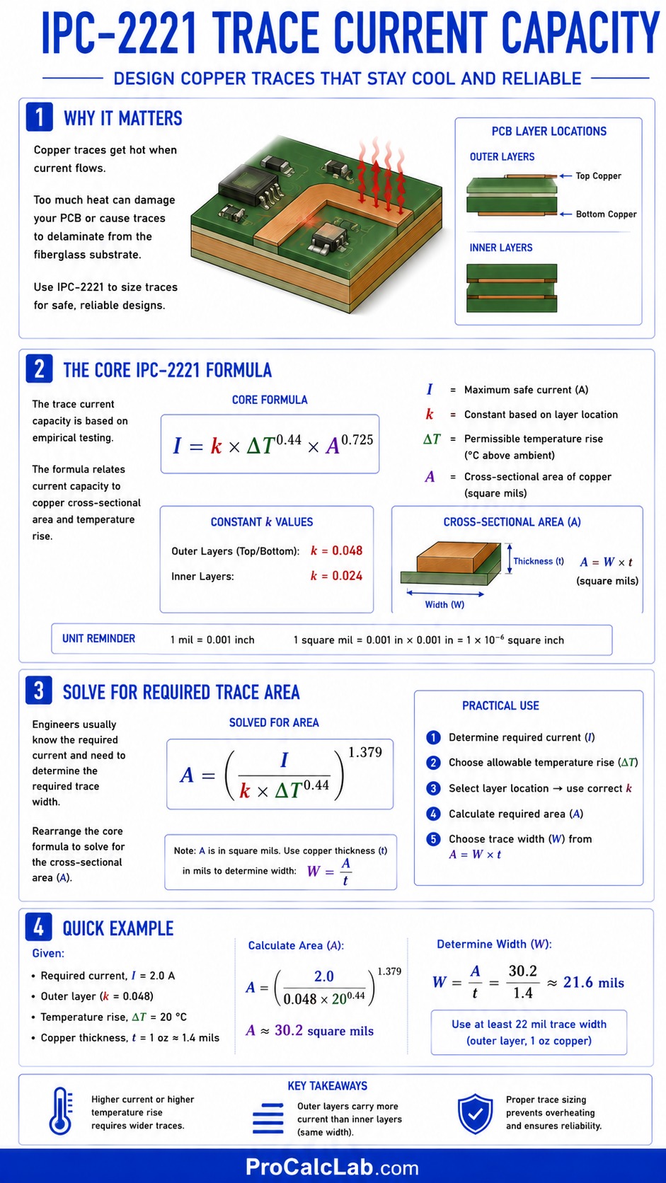
The fundamental equation for trace current capacity is highly empirical, derived from thousands of destructive tests. The core formula relates current capacity to the cross-sectional area of the copper and the allowable temperature rise.
The Core IPC-2221 Formula
I = k * ΔT0.44 * A0.725
Where the variables represent the following parameters:
- I is the maximum safe current in Amperes.
- k is a constant based on the layer location. It equals 0.048 for outer layers and 0.024 for inner layers.
- ΔT is the permissible temperature rise in degrees Celsius above ambient room temperature.
- A is the cross-sectional area of the copper trace in square mils.
Engineers usually know the required current and need to determine the required trace width. We must rearrange the equation to solve for the cross-sectional Area.
A = ( I / ( k * ΔT0.44 ) )1.379
A Real-World Trace Calculation
Imagine you are routing a primary power rail on the top outer layer of your board. The circuit demands 5 Amps of continuous current. You decide that a maximum temperature rise of 10 degrees Celsius is safe for your enclosure.
- Step is identifying your constant. Because this is an outer layer, k equals 0.048. The temperature rise ΔT equals 10.
- Step is solving the denominator. We calculate 10 to the power of 0.44, which equals 2.754. We multiply this by 0.048 to get 0.132.
- Step is dividing the current by our denominator. We divide 5 Amps by 0.132, yielding 37.87.
- Step is raising this result to the power of 1.379. Calculating 37.871.379 gives us a required cross-sectional area of 150.3 square mils.
To find the physical trace width, we divide the area by the thickness of the copper. Standard 1-ounce copper has a thickness of 1.37 mils. Dividing 150.3 by 1.37 tells us we need a trace width of exactly 109.7 mils to safely carry the 5 Amps. In your design software, you would round this up to 110 mils and route the connection. When you inspect the generated top copper Gerber file, you will see D-code commands drawing lines exactly 110 mils wide.
Copper Weight and Physical Thickness
The term copper weight is an antiquated but ubiquitous metric. It refers to the weight of 1 square foot of copper foil. A 1-ounce copper layer means that 1 square foot of that foil weighs exactly 1 ounce. This weight translates directly into a physical thickness, which is critical for both trace resistance calculations and impedance control for high-speed signals.
Standard Copper Weight to Thickness Metric
| Copper Weight Ounces | Nominal Thickness Millimeters | Application Note |
|---|---|---|
| 0.5 | 0.017 | Standard for inner signal layers. |
| 1.0 | 0.035 | Standard for top and bottom outer layers. |
| 2.0 | 0.070 | Used for heavy power supplies and motor drivers. |
| 3.0 | 0.105 | Extreme high current industrial applications. |
Standard Copper Weight to Thickness Imperial
| Copper Weight Ounces | Nominal Thickness Mils | Current Carrying Capacity Rating |
|---|---|---|
| 0.5 | 0.68 | Low current digital logic traces. |
| 1.0 | 1.37 | General purpose routing up to 2 Amps. |
| 2.0 | 2.74 | High current rails up to 10 Amps. |
| 3.0 | 4.11 | Massive thermal dissipation planes. |
Decoding the D-Codes
If you open a Gerber file in a raw text editor, you will see a massive block of alphanumeric strings. The letter D followed by a number is the most common command. These are known as D-codes or draft codes.
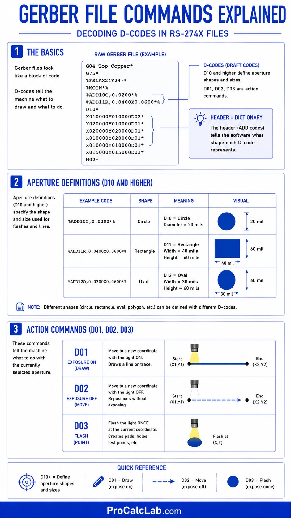
Commands ranging from D10 and higher define the shape and size of the aperture. For example, D10 might define a circle with a diameter of 20 mils. D11 might define a rectangle that is 40 mils wide and 60 mils tall. The header of the RS-274X file acts as a dictionary, explicitly telling the manufacturing software what shape each D-code represents. The commands D01, D02, and D03 are action commands. They tell the machine what to do with the currently selected aperture shape.
- D01: This is the exposure on command. It instructs the machine to move to a new coordinate while leaving the light beam turned on, effectively drawing a line or a trace.
- D02: This is the exposure off command. It instructs the machine to move to a new coordinate with the light beam turned off, repositioning the head without exposing any photoresist.
- D03: This is the flash command. It instructs the machine to flash the light beam exactly once at the current coordinate. This is used to create standalone shapes like component pads or test points.
The Excellon Drill File Connection
A Gerber archive is incomplete without the numerical control drill files, commonly referred to as Excellon files. While the Gerber files define where the copper sits, the Excellon file tells the automated drilling machines exactly where to plunge a tungsten carbide drill bit through the fiberglass panel.
📝 The drill file is critical because it dictates the plating process. Plated through-holes connect the top layer copper to the bottom layer copper by depositing a thin sleeve of copper down the inside of the drilled hole. Non-plated through-holes are used strictly for mechanical mounting hardware. The Excellon file lists the X and Y coordinates for every hole, categorizing them by the required drill bit diameter.
Drilling is a violent mechanical process. The spindle spins at speeds exceeding 100000 revolutions per minute. If you specify a via hole with a diameter of 0.2 millimeters on a board that is 1.6 millimeters thick, you are creating an aspect ratio of 8 to 1. Pushing chemical plating solutions through a hole this narrow relies entirely on capillary action. If the aspect ratio exceeds 10 to 1, standard fabrication houses cannot guarantee continuous copper plating inside the barrel of the via, leading to intermittent electrical failures in the field.
Real-World Troubleshooting at the Fab House
Understanding the theoretical files is only half the battle. The true test comes when you attempt to marry your digital data with physical manufacturing tolerances. Errors at this stage are unforgiving.
Solder Mask Swell and Expansion
Solder mask is a liquid epoxy applied over the entire board and cured with ultraviolet light. Because physical manufacturing is imperfect, the alignment of the solder mask layer to the copper layer will always have a slight registration offset. If you design the opening in your solder mask to be the exact same size as your copper pad, the inevitable slight shift will cause the mask epoxy to creep onto the edge of your pad. This severely impacts solderability.
To prevent this, engineers apply a solder mask expansion rule. Every opening in the mask must be physically larger than the copper pad beneath it by a margin of 2 to 4 mils. If your copper pad is 50 mils wide, the corresponding flash in the solder mask Gerber file should be 54 mils wide. This clearance ensures the entire copper pad remains exposed even if the machinery alignment drifts slightly during production.
Silkscreen Contamination on Solder Pads
The silkscreen layer applies the white text indicating component reference designators and polarity marks. Silkscreen ink is an electrical insulator. If your Gerber files instruct the printer to lay ink directly on top of an exposed surface mount pad, the solder paste will not stick to the copper during the reflow process. The component will literally fall off the board.
Before exporting, you must run a strict design rule check ensuring all silkscreen elements are pulled back at least 3 mils from any exposed copper geometry. Many advanced fabrication houses run automated scripts to clip any ink that violates this rule, but relying on the manufacturer to fix your geometry errors is a dangerous and unprofessional habit.
Validating Your Fabrication Data
Validating your files before ordering is a mandatory step. Instead of blindly trusting the export dialog, you must review the generated layers independently. We highly recommend using our 2D/3D PCB Design & Gerber File Viewer to overlay your drill files against your copper layers. This specific tool allows you to visually catch offset errors where the via holes miss the copper pads entirely, preventing disastrous manufacturing defects.
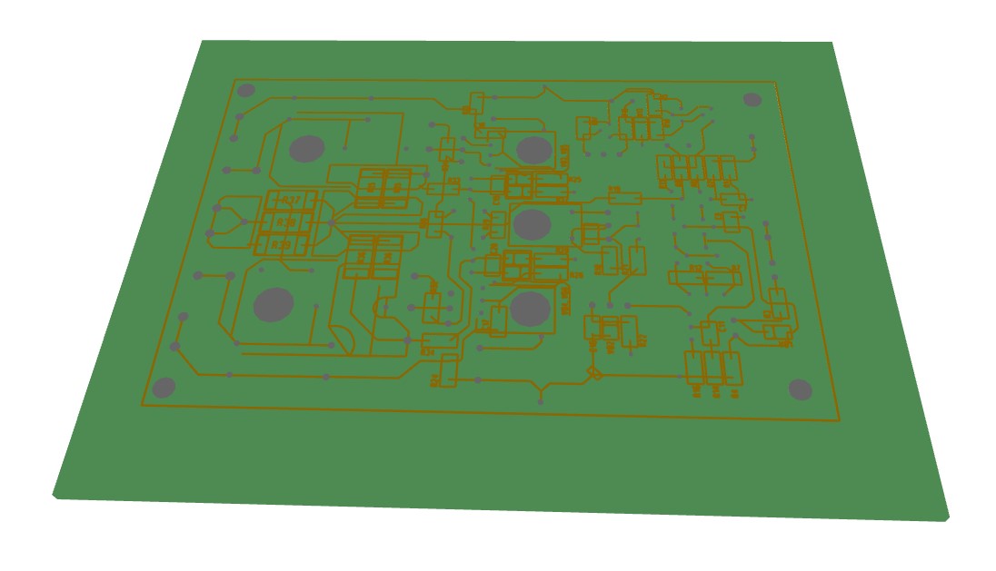
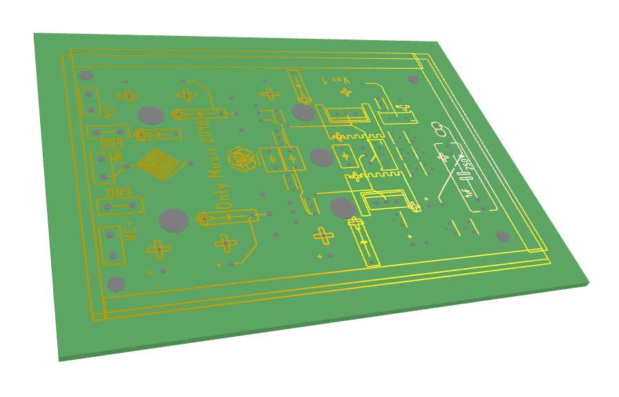
By loading the top copper, bottom copper, and the Excellon drill file into a neutral viewer, you strip away the comforting illusions of your design software. You see exactly what the photoplotter and CNC drill will see. Check your board outlines. A missing mechanical outline layer means the factory router has no path to follow to cut your individual board out of the larger manufacturing panel. The production line will instantly halt, costing you days of delay.
Final Verification and Structural Integrity
A printed circuit board is a mechanical structure first and an electrical circuit second. It must survive thermal shock during the reflow soldering process, resist mechanical vibration in its final enclosure, and maintain electrical isolation under varying humidity levels. The Gerber files are the literal blueprints for this mechanical structure.
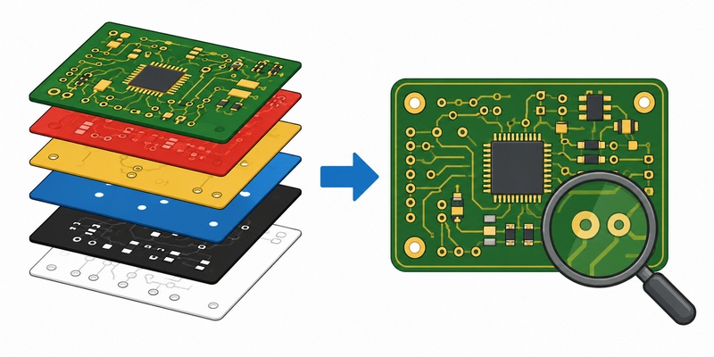
By understanding that a flash command builds a pad and a draw command builds a trace, you take total control over the manufacturing process. You stop guessing why your trace width calculations failed and start designing robust, manufacturable hardware that survives the transition from pixels on a screen to physical copper in your hands.
Literature and Reference Standards
To design structures that comply with modern manufacturing capabilities, engineers must rely on rigorous international specifications. The physics of current capacity and file formatting are strictly governed by the following documents.
- IPC-2221B, Generic Standard on Printed Board Design. This document provides all the foundational mathematics for trace spacing, voltage clearances, and current carrying capacity.
- IPC-A-600K, Acceptability of Printed Boards. This manual outlines the visual and mechanical criteria for accepting or rejecting a fabricated bare board.
- Ucamco RS-274X Gerber Format Specification. The definitive technical manual detailing the ASCII structure, aperture macros, and coordinate data formatting for all modern photoplotters.
- IPC-7351C, Generic Requirements for Surface Mount Design and Land Pattern Standard. This establishes the mathematics for calculating optimal pad geometries and solder mask expansions.

David Parry — Senior Engineering Analyst
Specializing in electronics and physics-based simulations with 20+ years of engineering experience. David ensures the mathematical and physical accuracy of the tools at ProCalcLab.