
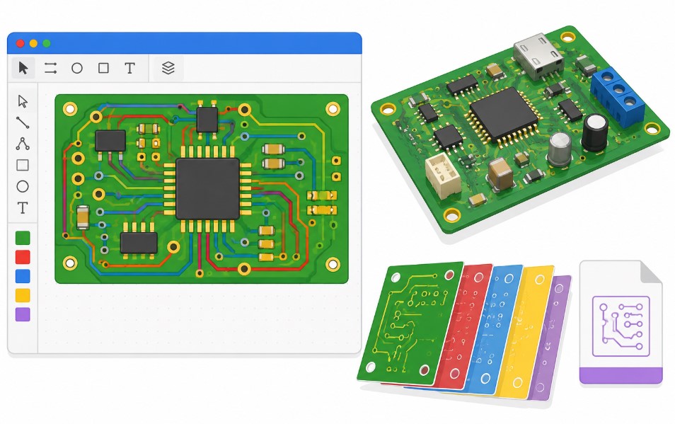
Printed circuit boards form the foundation of almost every modern electronic device. Before a board goes into physical production, factories require a standardized set of digital blueprints. These blueprints dictate exactly where copper traces run, where holes need drilling, and what areas receive a protective coating. Inspecting these files visually is a critical step to prevent costly manufacturing errors. This browser-based visualization tool provides an immediate, clear look at board designs without requiring heavy desktop software installations.


The system renders standard manufacturing files directly on the screen. It translates raw coordinate data into a highly accurate physical representation. Users can toggle between flat flat perspectives and fully rotatable three-dimensional models. This ensures all contact pads align perfectly and drill holes correctly penetrate the board material.
Table of Contents
How to Use the Visualization Tool
Operating the viewer requires no specialized engineering background. The interface focuses on essential controls to keep the inspection process straightforward.
Uploading Board Files
The primary action involves loading the design data. The system accepts individual layer files or complete compressed archives. Compressing all exported manufacturing files into a single ZIP archive is the most efficient method. When a ZIP archive is uploaded, the tool automatically unpacks the contents, identifies the purpose of each layer based on its file extension, and stacks them in the correct physical order. The loading indicator displays the file name once processing completes.
Navigating the 3D Space
Once the board appears on the screen, users can manipulate the camera to inspect details. Clicking and dragging the cursor across the board rotates the model in 3D space. Scrolling the mouse wheel zooms the view in and out for close-up inspections of tiny copper traces. The tool includes a dedicated zoom slider at the bottom of the screen for precise magnification adjustments. A dedicated button automatically centers the board and scales it to fit perfectly within the viewing area.
Switching Viewing Modes
Different inspection tasks require different perspectives. The tool features a primary toggle button to switch between two-dimensional and three-dimensional rendering. The 2D mode provides a traditional flat top-down view, which is excellent for checking text legibility and general component placement. The 3D mode adds physical depth, showing the actual thickness of the board substrate and how drill holes pass through the material.
Controlling Visibility and Environment
A complex board often contains overlapping layers that obscure important details. The layer toggle function isolates specific parts of the design. Users can cycle the view to show all layers combined, only the top side elements, or solely the bottom side elements. This helps verify that bottom-layer traces do not interfere with top-layer components.
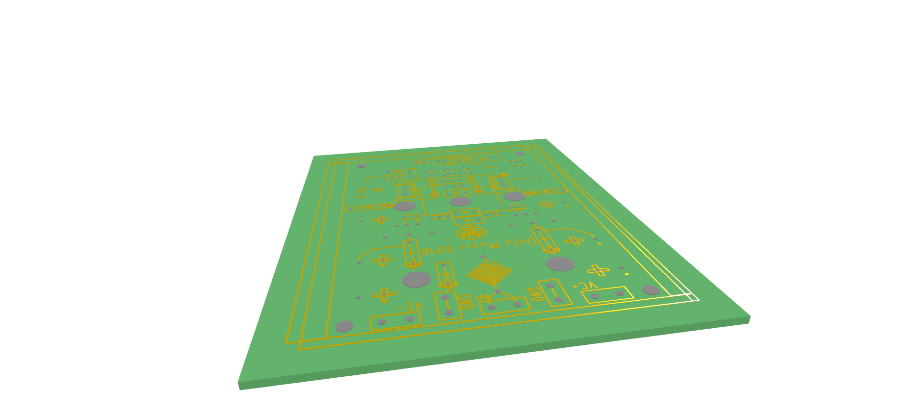
Environmental controls further enhance the inspection process. A grid overlay can be activated to provide a sense of scale and proportion. For better visual contrast, the ambient light intensity slider adjusts the overall brightness of the scene. Additionally, the mask color selector allows changing the simulated board material color. While green is the traditional default, viewing the design in blue, black, or red can sometimes highlight missing copper areas more effectively.
Capturing and Displaying Options
Documenting a design issue or sharing the layout with a client requires saving the visual output. The screenshot button instantly captures the current camera view and downloads it as a high-quality image file. For complex boards requiring maximum screen real estate, the full-screen mode expands the viewing canvas to cover the entire monitor, hiding browser toolbars and other distractions.
Understanding Manufacturing File Formats
The tool processes standard vector format files used universally by the electronics manufacturing industry. These text-based files contain coordinate lists and tool commands. They tell the factory machines exactly where to move, flash light, or drill down. Because different design software packages use varying naming conventions, understanding common file extensions helps clarify what is being uploaded.
| File Extension | Layer Type | Primary Purpose |
|---|---|---|
| .GTL | Top Copper | Defines the metal traces and pads on the top surface. |
| .GBL | Bottom Copper | Defines the metal traces and pads on the bottom surface. |
| .GTS | Top Solder Mask | Protective coating area to prevent solder bridges on top. |
| .GBS | Bottom Solder Mask | Protective coating area to prevent solder bridges on bottom. |
| .GTO | Top Silkscreen | White ink text and component outlines on the top side. |
| .GBO | Bottom Silkscreen | White ink text and component outlines on the bottom side. |
| .GKO | Board Outline | The physical outer boundary and routing path of the board. |
| .DRL | Drill Data | Coordinates and tool sizes for making physical holes. |
| .TXT | Drill Data Alternative | Often used interchangeably with standard drill formatting. |
| .GM1 | Mechanical Layer | Additional dimensions or internal routing paths. |
Standard Board Specifications
When preparing designs for visual inspection and eventual manufacturing, certain physical properties remain consistent across the industry. Factories optimize their production lines around specific baseline measurements. Straying from these standard numbers usually increases production costs and lead times. The viewer simulates the board based on these common industry defaults to provide a realistic digital twin.
| Physical Parameter | Standard Value | Advanced Value |
|---|---|---|
| Substrate Thickness | 1.6 mm | 0.8 mm |
| Copper Weight | 1 oz | 2 oz |
| Minimum Trace Width | 6 mil | 4 mil |
| Minimum Clearance | 6 mil | 4 mil |
| Solder Mask Clearance | 2 mil | 1 mil |
| Silkscreen Line Width | 5 mil | 3 mil |
| Silkscreen Text Height | 30 mil | 20 mil |
| Via Hole Size | 0.3 mm | 0.2 mm |
| Via Pad Diameter | 0.6 mm | 0.4 mm |
| Board Edge Clearance | 10 mil | 5 mil |
Drill Holes and Tooling
Holes play a dual role in board design. They either provide a physical mounting point for a component leg or establish an electrical connection between different copper layers. The latter are known as vias. The viewer meticulously renders these holes to ensure they align perfectly with the surrounding copper pads. Missing drill files are a common issue; without them, the board will appear solid, and the factory will not know where to bore through the fiberglass.
| Hole Category | Typical Diameter | Manufacturing Application |
|---|---|---|
| Standard Microvia | 0.2 mm | High-density connections between adjacent layers. |
| Standard Via | 0.3 mm | Basic electrical routing from top to bottom. |
| Small Component Lead | 0.6 mm | Resistor and capacitor wire leads. |
| Medium Component Lead | 0.8 mm | Integrated circuit pins and standard headers. |
| Large Component Lead | 1.0 mm | Power connectors and heavy-duty switches. |
| Small Mounting Hole | 2.0 mm | Miniature enclosure standoff screws. |
| Standard Mounting Hole | 3.2 mm | Common hardware screws for securing the board. |
| Tooling Hole | 4.0 mm | Alignment pins for factory assembly machines. |
Practical Benefits of Pre-Production Visualization
A digital visual check serves as the final quality control gateway. Raw data files look like endless strings of numbers and coordinates in a text editor. Human eyes cannot parse these numbers to find design flaws. Translating the data back into a visual medium highlights obvious and subtle errors immediately.
- One primary benefit is verifying layer alignment. Occasionally, design software might export a bottom layer mirrored or offset by several inches. In a 3D visualization, this error becomes glaringly obvious as the drill holes will float entirely outside the copper paths. Catching an offset error before sending the files to a fabrication house prevents the total loss of the manufacturing run.
- Another major advantage involves checking the solder mask expansion. The mask is the colored layer that protects the board. It needs small openings around every metal pad so solder can stick to the copper. If the mask file is generated incorrectly, it might cover the pads completely. A visual inspection clearly shows whether the metal pads are exposed or buried beneath the protective coating.
- Finally, visual inspection helps identify missing layers. If an uploaded archive lacks an outline file, the viewer cannot determine where the board ends, often resulting in an infinitely stretching substrate or a strange bounding box. Spotting this anomaly prompts a quick re-export from the design software, ensuring the factory receives a complete blueprint package.
Troubleshooting Common Issues
While the viewer is designed to handle a wide array of formats automatically, some poorly formatted exports can cause display anomalies. Understanding the root causes of these visual glitches speeds up the correction process.
If the entire board appears microscopic or gigantic on the screen, the issue usually stems from missing scale declarations in the original file. Older export formats sometimes fail to specify whether the coordinates are in millimeters or inches. The rendering engine attempts to guess based on standard parameters, but manual correction in the design software settings is the best permanent fix.
When copper traces appear completely disconnected or jagged, the problem likely involves unsupported aperture definitions. An aperture dictates the shape of the drawing tool round, square, or custom. If a design relies heavily on complex custom shapes that the standard parser cannot translate, the drawn lines may break. Simplifying the shape rules before exporting usually resolves visual jaggedness.
If the viewer loads endlessly or the browser becomes unresponsive, the uploaded file might be exceptionally dense. Boards with massive poured copper regions defined by thousands of tiny overlapping lines rather than solid polygons require immense processing power to draw. Switching the design software to export copper pours as solid polygons drastically reduces file size and load times.
Summary of Best Practices
Achieving the best results with any visual inspection tool relies on clean initial data. Always ensure that the design software is configured to use the latest RS-274X standard rather than the obsolete standard that requires separate tool definition files. Export all files simultaneously into a single dedicated folder to prevent mixing old and new versions. Name the files logically, or rely on the software default extensions, so the parser can easily identify the top copper from the bottom copper. By following these straightforward data management rules, the visualization process remains rapid, accurate, and highly informative.
Reference Literature
- Ucamco Gerber Format Specification Manual. Detailed syntax and parameter guidelines for RS-274X vector image formats.
- Printed Circuit Board Design Guidelines. Standard clearance and manufacturing tolerances for rigid substrates.
- Excellon Drill Format Reference. Syntax rules for automated drilling machines and coordinate mapping.
- Web Audio and Canvas Rendering Documentation. Best practices for 2D and 3D geometric translations in modern browser environments.
- Modern Electronics Fabrication Processes. An overview of chemical etching, masking, and automated optical inspection workflows.

David Parry — Senior Engineering Analyst
Specializing in electronics and physics-based simulations with 20+ years of engineering experience. David ensures the mathematical and physical accuracy of the tools at ProCalcLab.


