Desktop electronic design automation software often demands a steep learning curve and significant system resources. Large design suites require complex netlist creation, schematic capture, component footprint assignment, and strict design rule verification before a designer can draw a single track. For simple hobby projects, educational demonstrations, quick conceptual sketches, or hardware documentation, a lightweight browser utility provides an immediate alternative. By working inside a responsive layout constrained to a maximum width of 340 pixels, this online creator ensures that all board designs remain perfectly readable across mobile viewports, responsive web forums, and technical blogs.
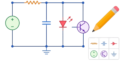
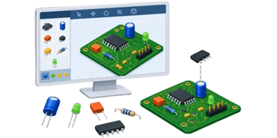

✍ This reference manual explains how to interact with the layout tool, outlines fundamental printed circuit board design rules, provides essential estimation formulas, and presents curated layout data tables. The focus remains on quick, practical reference information rather than deep academic theory.
Table of Contents
Step-by-Step Layout Tool Reference
The layout creator interface contains three primary sections: the top tool selection strip, the central interactive canvas, and the bottom control panel. Understanding how these elements interact helps users sketch clean, export-ready board designs efficiently.
The Component and Drawing Toolbar
The top toolbar provides the active drawing tools required to build a physical board layout. Clicking any tool highlights its button and changes the action performed on the canvas.
- Circle Tool: Used to sketch round component outlines, bulk capacitors, circular board mounting holes, or test points.
- Line Tool: Draws standard signal traces. This tool places straight lines connecting component pads. It is also useful for defining physical board boundaries.
- Point Tool: Places small circular pads. These represent small through-hole terminals, wire connection points, or circuit vias that link different routing paths.
- Arrow Tool: Draws directional indicators. This tool is intended for documentation purposes, helping to point out specific circuit nodes, signal directions, or test areas for assembly manuals.
- Vertical Pad Tool: Places a vertically oriented rectangular contact pad. These are commonly used for standard dual-in-line integrated circuit pins, vertical resistor placements, or header connectors.
- Horizontal Pad Tool: Places a horizontally oriented rectangular contact pad. This is ideal for standard horizontal resistors, surface-mount diodes, or axial-lead capacitors.
- Text Tool: Opens a text entry prompt to place labels directly onto the board surface. Use this tool for component designators like R1 or C1, polarity markings, input/output labels, or project titles.
The Canvas Workspace
The center canvas features a fixed layout boundary that scales perfectly down to mobile screens. Clicking and dragging inside this area applies the currently selected tool. The cursor changes to a crosshair to indicate precise targeting. When an element is placed, the application keeps track of its specific coordinates in the background, allowing for automated alignment adjustments and clean graphic exports.
The Bottom Control Panel Actions
The lower control panel provides management and file export operations. These buttons utilize vector graphics instead of heavy raster images to maintain fast page loading times.
- Clear All: Completely flushes the canvas memory, removing every element and resetting the workspace to a blank white sheet. This action cannot be undone.
- Undo: Step-by-step history reversal. This function removes the very last element placed on the board, allowing users to correct drawing mistakes without touching the rest of the layout.
- Delete Item: Removes targeted components or traces that are currently active or highlighted, keeping the surrounding layout safe.
- Export SVG: Generates a Scalable Vector Graphics file of the drawing. This format preserves infinite resolution scalability, making it the perfect choice for importing into professional graphics software or vector-based documentation editors.
- Export Transparent PNG: Renders the current layout as a standard raster image with a clear background alpha channel. This file type is ideal for overlaying circuit layouts onto colored documentation web pages, dark-mode presentations, or forum posts.
- Export White BG PNG: Saves a raster image with a solid white background block. This output matches classic printing standards and technical manuals that require high-contrast physical printouts.
- Fullscreen Mode: Maximizes the layout box to fill the entire monitor or phone screen. This modal view expands user control, centers the 340-pixel drawing interface, and removes background clutter for highly accurate touch-screen or mouse interactions.
Practical Printed Circuit Board Layout Principles
When translating a physical schematic diagram into a real circuit board layout using a basic drawing tool, several layout rules prevent electrical and mechanical failures. While advanced software enforces these rules automatically, manual sketching requires a conscious effort to follow basic engineering standards.
Trace Geometry and Signal Flow
When drawing copper tracks with the Line Tool, sharp 90-degree corners must be avoided. Sharp right angles create abrupt changes in track width, which can lead to manufacturing defects during chemical copper etching. The acid used in production can become trapped in sharp inner corners, eating away too much copper and creating a high-resistance bottleneck or a complete open circuit. Instead, use two 45-degree turns to change direction. This approach maintains a consistent track width and ensures a smooth current flow throughout the board system.
Pad Placement and Footprint Integrity
Component pads must be placed with adequate spacing to prevent solder bridging during assembly. A solder bridge occurs when molten solder accidentally connects two adjacent pads, creating a short circuit. When laying out integrated circuits using the Vertical Pad Tool, maintain a uniform gap between pins. Additionally, ensure that through-hole component leads have large enough pads to provide mechanical stability. Components that experience physical stress, such as connectors, switches, and large capacitors, require larger pad areas to prevent the copper from peeling away from the underlying fiberglass board material.
Essential Board Estimation Formulas
When designing a quick layout, calculating trace characteristics prevents overheating and voltage drop issues. These simple formulas use basic geometric properties to estimate electrical behavior before manufacturing begins.
Trace Resistance Formula
The electrical resistance of a copper track depends on its temperature, length, width, and thickness. To find the resistance of a straight trace, use the following structural formula:
R = ρ × L / (W × T)
Where the variables represent the following physical properties:
- R: Trace resistance measured in Ohms.
- ρ: Resistivity of copper, which is approximately 0.0000000172 Ohm-meters at normal room temperature.
- L: Total length of the trace line.
- W: Width of the trace line.
- T: Thickness of the copper layer on the board.
Trace Voltage Drop Estimation
When high current passes through a narrow board track, resistance causes a drop in voltage by the time the signal reaches the destination component. Calculate this drop using Ohm’s Law:
Vdrop = I × R
Where the variables denote:
- Vdrop: Voltage lost along the track, measured in Volts.
- I: Current flowing through the track, measured in Amperes.
- R: Total trace resistance calculated from the trace resistance formula.
Trace Power Dissipation
Electrical energy lost due to trace resistance is converted directly into heat. To determine how much power a specific track must dissipate, use the power loss equation:
Ploss = I2 × R
Where the values indicate:
- Ploss: Power lost as heat, measured in Watts.
- I: Electrical current in Amperes.
- R: Trace resistance in Ohms.
Reference Data Tables for Layout Planning
The following tables provide rounded reference values based on standard industry design metrics. These tables help determine pad sizes, trace widths, and copper specifications during the quick sketching process.
Trace Width and Current Carrying Capacity
This table outlines the recommended trace width values for a standard board containing 1.4 mils of copper thickness, which corresponds to the common one-ounce copper specification, assuming a safe temperature rise of 10 degrees Celsius.
| Trace Width in Mils | Maximum Current in Amperes | Typical Application Type |
|---|---|---|
| 10 | 0.5 | Low-power digital signals and logic routing |
| 15 | 0.8 | Standard microcontroller pins and data busses |
| 20 | 1.2 | Low-power analog lines and LED indicators |
| 30 | 1.8 | Medium power distribution tracks |
| 50 | 2.6 | Main power supply rails for small circuits |
| 70 | 3.5 | High-current DC motor driver outputs |
| 100 | 4.5 | Heavy-duty power entry and ground return tracks |
Common Component Pad Pitch and Spacing
When sketching component footprints manually on the canvas, matching standard component pin intervals is vital for smooth physical assembly. Pitch is defined as the distance from the center of one pad to the center of the next adjacent pad.
| Component Package Type | Standard Pitch Distance | Layout Arrangement Tip |
|---|---|---|
| Dual In-Line Package ICs | 2.54 mm | Align two rows of vertical pads perfectly parallel |
| 0805 Surface Mount Devices | 2.00 mm | Use two horizontal pads facing each other closely |
| 1206 Surface Mount Devices | 3.20 mm | Provides wider spacing for easy manual hand soldering |
| TO-220 Power Transistors | 2.54 mm | Leave extra clearance around pads for a metal heatsink |
| Standard Quarter-Watt Resistors | 7.62 mm | Space pads far enough apart for clean component lead bending |
| Small Signal Diodes | 5.08 mm | Always check the text label orientation for correct polarity |
Copper Weight and Thickness Reference
Circuit board manufacturers measure copper foil thickness by weight in ounces per square foot. This table shows the real physical thickness conversions rounded to reasonable practical limits.
| Copper Weight Rating | Thickness in Mils | Common Workspace Environment |
|---|---|---|
| 0.5 oz per square foot | 0.7 | High-density smartphone circuits and fine pitch layouts |
| 1.0 oz per square foot | 1.4 | Standard consumer electronics and general hobbyist projects |
| 2.0 oz per square foot | 2.8 | Industrial power supplies and high-load relay boards |
| 3.0 oz per square foot | 4.2 | Heavy-duty automotive electronics and power inverters |
Layout Optimization Tips for Web Documentation
If the sketched board diagram is intended for a blog post, an instructional manual, or an online tutorial, visual clarity is just as important as electrical correctness. Follow these layout habits to create professional web graphics:
- Keep Text Readable: Use the Text Tool to label all critical ports. Place text outside the component body outlines so that physical parts do not block the labels during assembly demonstrations.
- Incorporate Clear Polarity: For components like electrolytic capacitors and diodes, use text markers or small point arrays to clearly identify positive and negative terminals. This practice prevents component damage during actual physical board assembly.
- Utilize Transparent Exports Smartly: When exporting files for websites featuring adaptive dark and light display modes, choose the Transparent PNG option. This allows the background grid lines of the webpage theme to blend naturally with the circuit graphic, preventing bright white layout blocks from breaking the webpage design.
- Establish a Consistent Ground Strategy: Dedicate a wide, continuous path along the edge of the layout sketch to serve as the main ground connection. A thick ground line minimizes electrical noise and simplifies the connection of multiple sub-circuits.

Literature and Useful Sources
- Association Connecting Electronics Industries. IPC-2221B: Generic Standard on Printed Board Design. IPC, 2012.
- Brooks, Douglas. Signal Integrity Issues and Printed Circuit Board Design. Prentice Hall, 2003.
- Khandpur, Raghbir Singh. Printed Circuit Boards: Design, Fabrication, Assembly and Testing. McGraw-Hill Education, 2005.
- Hartley, Rick. Control of Noise, EMI, and Signal Integrity in Practical PCB Layouts. MediaIsis, 2018.

David Parry — Senior Engineering Analyst
Specializing in electronics and physics-based simulations with 20+ years of engineering experience. David ensures the mathematical and physical accuracy of the tools at ProCalcLab.