
Early in my career working for an aerospace contractor, I spent 3 days waiting for the IT department to provision a high-performance workstation and secure a $15,000 floating software license simply so I could design a 2-layer breakout board for a new pressure transducer. The actual design work took less than 45 minutes. The administrative overhead and software loading times took 72 hours. This massive friction is a known killer of engineering momentum. When a designer is forced to navigate complex licensing servers, heavy local installations, and overwhelming enterprise menus just to verify a component footprint or draft a conceptual circuit, the creative iteration cycle grinds to a halt.


In the field, we often see engineering teams bottlenecked by their own powerful tools. Desktop electronic design automation suites are incredibly robust for routing 16-layer high-speed digital motherboards. However, they are entirely the wrong tool for testing a simple analog filter, documenting a hardware hack, or teaching junior engineers the basics of signal flow. We need accessible environments where ideas can transition into physical geometry without a steep learning curve. By shifting the initial printed circuit board design phase into a lightweight web browser environment, we strip away the bloat and return focus to the core mechanics of electrical engineering.
🎓 This article details the underlying physics of printed circuit board layout, the mathematical models required for sizing traces safely, the logic behind rendering geometric data in a browser, and practical techniques for ensuring your rapid prototypes are highly manufacturable.
Table of Contents
The Mechanics of Web-Based Board Layout
Designing a circuit board is fundamentally an exercise in 2D coordinate geometry and boolean operations. You are placing copper polygons on a fixed grid and ensuring they maintain minimum spatial clearances from each other to prevent electrical arcing. When we transition this process from a compiled desktop application to a browser utility, we rely on the graphics rendering pipeline of the browser itself using technologies like WebGL and Scalable Vector Graphics.
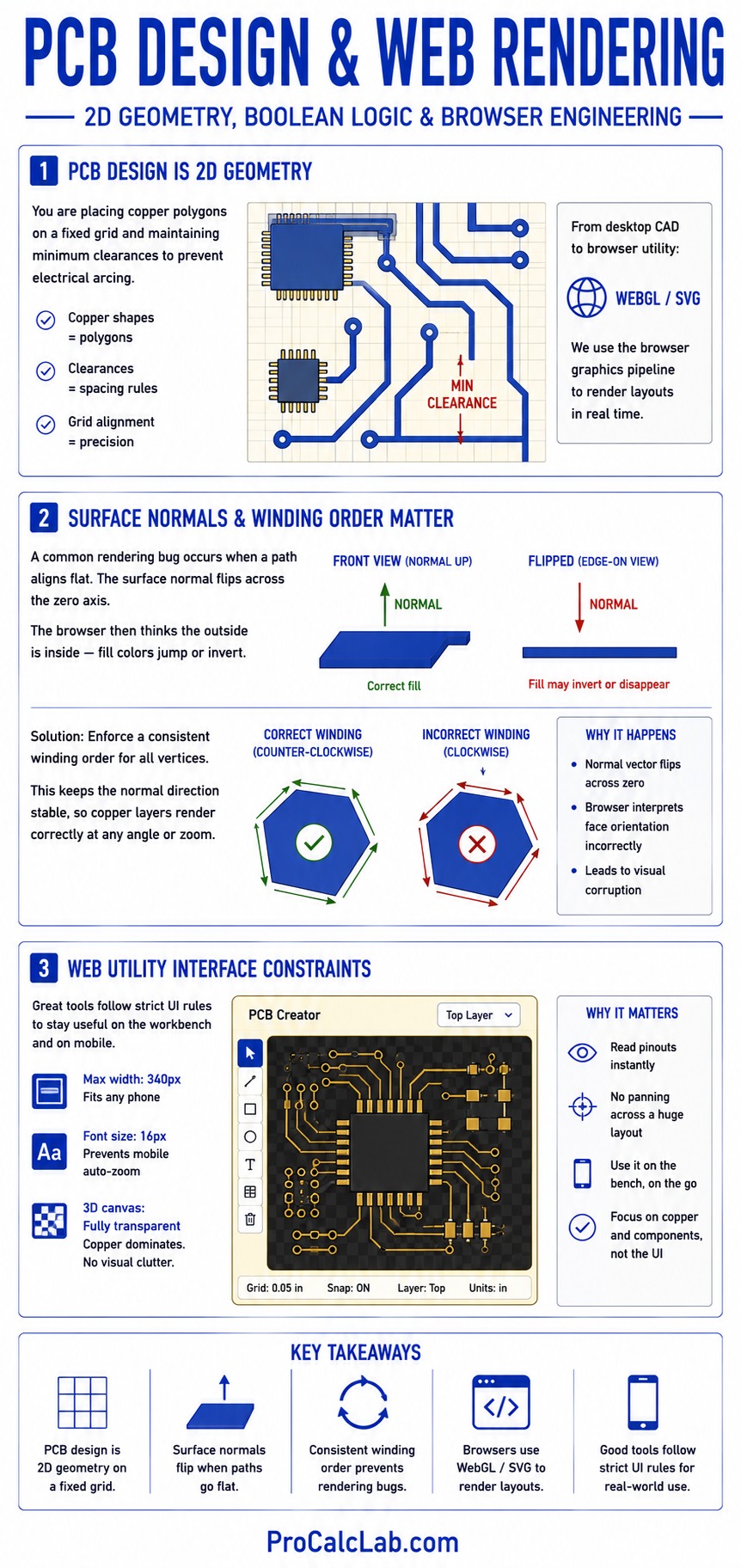
A common mistake during calculations for web rendering involves the mathematical surface normals of the polygon paths. I have reviewed SVG animation logic from various developers where automated fill colors jump abruptly or switch completely when a path aligns to a flat orientation. This rendering glitch occurs because the surface normal vector flips across the zero axis, causing the browser engine to interpret the outside face of the copper trace as the inside face. To prevent this visual corruption, the underlying layout engine must strictly enforce a persistent mathematical winding order for all vertices. This ensures the copper layers render perfectly regardless of the viewing angle or zoom level.
Beyond rendering physics, web utilities must adhere to strict interface constraints to remain genuinely useful. When drafting these initial layouts, we rely on tools like our browser PCB creator because it forces discipline. You can pull the tool up on a mobile phone while standing over a workbench and read the exact pinout of a microcontroller without panning endlessly across a screen.
The Mathematics of Trace Current Capacity
Even in a lightweight rapid prototyping environment, the immutable laws of physics apply. When you route a copper trace between 2 components, that trace acts as a resistor. As current flows through this resistor, it dissipates power in the form of heat. If the trace is too narrow, the heat will rapidly exceed the glass transition temperature of the fiberglass substrate, causing the board to delaminate, burn, and ultimately fail.
✍ To determine the exact required width of a copper trace, engineers use empirical mathematical models established by the IPC-2221 standard. This standard provides a method to calculate the cross-sectional area of copper required to carry a specific current while keeping the temperature rise below a strictly defined threshold.
The core equation governing the required cross-sectional area A in square mils is:
A = (I / (k * ΔTb))1/c
Let us break down the variables governing this physical relationship:
- A: The required cross-sectional area of the copper trace measured in square mils.
- I: The continuous electrical current measured in Amperes.
- ΔT: The maximum allowable temperature rise above ambient room temperature measured in degrees Celsius.
- k, b, c: Empirical constants derived from decades of thermodynamic testing. For external copper layers exposed to air, k is 0.048, b is 0.44, and c is 0.725.
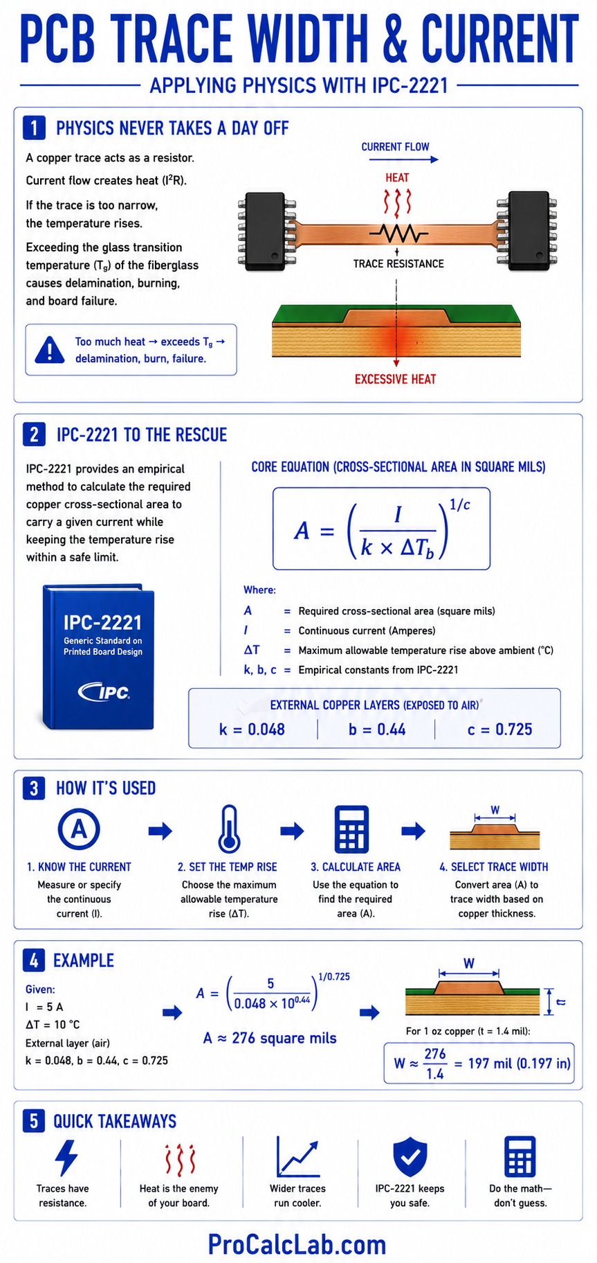
Let us walk through a concrete calculation. We are designing a power distribution board for a custom robotics project. We need to route a main power trace carrying exactly 5 Amps of continuous current. We want to ensure the trace does not heat up more than 10 degrees Celsius above the ambient air. We are routing this on the top external layer of the board.
First, we plug our known values into the IPC equation. The exponent 1 divided by 0.725 simplifies to approximately 1.38.
A = (5 / (0.048 * 100.44))1.38
We begin by solving the temperature rise factor.
100.44 = 2.754
Next, we multiply this by our external layer constant k.
0.048 * 2.754 = 0.132
Now we divide our 5 Amp current requirement by this denominator.
5 / 0.132 = 37.88
Finally, we raise this result to the power of 1.38 to find the required cross-sectional area.
A = 37.881.38
A = 154.2 square mils.
This tells us the sheer volume of copper required, but we design boards in 2 dimensions using trace width. We must divide this area by the physical thickness of the copper foil on our board. Standard prototyping boards use 1-ounce copper, which translates to a physical thickness of exactly 1.37 mils.
Trace Width = 154.2 / 1.37
Trace Width = 112.5 mils.
If you route that 5 Amp power line using a default 10 mil signal trace in your browser utility, the copper will act as a fuse, instantly vaporizing the moment you apply power. Understanding this math allows you to design safe hardware before writing a single line of firmware.
Calculating Trace Resistance and Voltage Drop
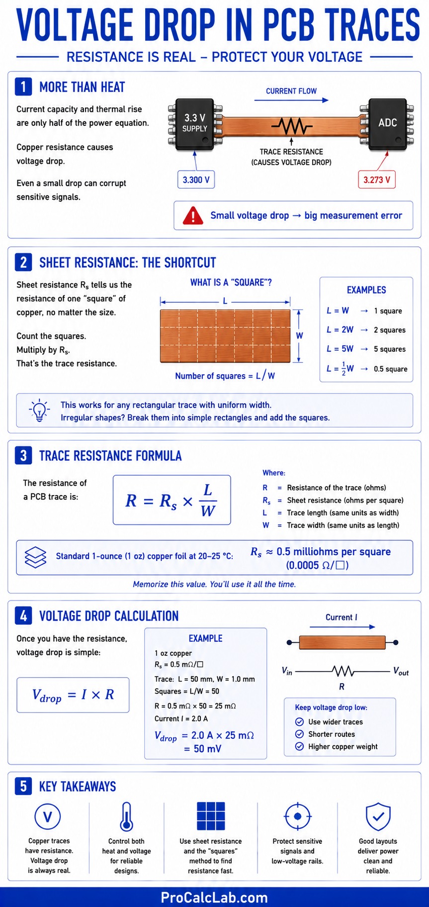
Current capacity and thermal rise are only half of the power equation. The other critical factor is voltage drop. Because the copper trace possesses intrinsic electrical resistance, a portion of your supply voltage will be lost along the length of the layout. If you are routing a sensitive 3.3 Volt reference signal to an analog-to-digital converter, a tiny voltage drop can severely corrupt your sensor readings.
📉 To calculate this, we use the standard sheet resistance formula. Sheet resistance Rs is a powerful engineering shortcut that allows us to calculate the resistance of any rectangular trace simply by counting how many squares of copper fit inside it, regardless of the physical size of those squares.
The resistance R of a trace is calculated as:
R = Rs * (L / W)
Where L is the physical length of the trace and W is the physical width. For standard 1-ounce copper foil at room temperature, the sheet resistance Rs is approximately 0.5 milliohms per square. This value is a constant you should memorize.
Let us return to our previous example. We have a trace that is 112.5 mils wide. Let us assume we have to route this trace across the entire length of the circuit board, a distance of 2000 mils.
First, we determine the number of squares in our trace by dividing the length by the width.
Squares = 2000 / 112.5
Squares = 17.77
Now we multiply the number of squares by our 1-ounce copper sheet resistance constant.
R = 17.77 * 0.0005 ohms
R = 0.0088 ohms
Our power trace has a total end-to-end resistance of 0.0088 ohms. To find the exact voltage drop V across this trace, we apply Ohm’s Law, multiplying our 5 Amp current by our calculated resistance.
V = 5 * 0.0088
V = 0.044 Volts.
In a 5 Volt logic system, losing 0.044 Volts as heat along a power rail is generally acceptable. However, if this trace were routing a low-voltage high-current supply to a modern processor core running at 1 Volt, dropping nearly 50 millivolts could easily push the processor out of its stable operating window. From a practical standpoint, always calculate voltage drop on long power runs, even on simple 2-layer prototypes.
Standard Copper Weights and Sheet Resistance
The calculations above rely heavily on the physical thickness of the copper clad to the fiberglass substrate. The printed circuit board industry measures this thickness in ounces, representing the weight of 1 square foot of copper rolled flat. The following table provides the critical dimensions and electrical properties for common manufacturing standards. We present both Imperial and Metric values combined logically to prevent conversion errors when sending browser-generated GERBER files to international fabrication houses.
| Copper Weight, oz/ft2 | Foil Thickness, mils / mm | Sheet Resistance, mΩ/sq |
|---|---|---|
| 0.5 | 0.68 / 0.017 | 1 |
| 1 | 1.37 / 0.035 | 0.5 |
| 2 | 2.74 / 0.07 | 0.25 |
| 3 | 4.11 / 0.104 | 0.17 |
Dielectric Spacing and Electrical Clearance
While trace width dictates how much current a layout can safely handle, trace spacing dictates what voltage the layout can safely withstand. If you place 2 copper traces too close together, a high voltage differential will ionize the air or the fiberglass substrate between them, creating a catastrophic electrical arc.
📊 We classify this spacing into 2 categories: clearance and creepage. Clearance is the shortest distance through the air between 2 conductive parts. Creepage is the shortest path along the physical surface of the insulating substrate between 2 conductive parts. When routing a board, we primarily concern ourselves with creepage along the FR4 fiberglass surface.
The IPC-2221 standard dictates strict minimum spacing rules based on the peak voltage difference between any 2 adjacent traces. Internal layers can tolerate tighter spacing because the copper is fully encapsulated in cured epoxy resin, completely eliminating air and moisture. External layers require significantly wider gaps.
| Peak Voltage, V | Internal Layer Clearance, mils / mm | External Layer Clearance, mils / mm |
|---|---|---|
| 0 to 15 | 2 / 0.05 | 4 / 0.1 |
| 16 to 50 | 4 / 0.1 | 24 / 0.6 |
| 51 to 100 | 4 / 0.1 | 24 / 0.6 |
| 101 to 250 | 8 / 0.2 | 49 / 1.25 |
Notice the massive jump in external clearance requirements once you exceed 15 Volts. If you are using a rapid browser utility to design a circuit controlling a 120 Volt alternating current relay, you cannot simply use a default 10 mil grid snap for your routing. You must manually ensure at least 49 mils of bare fiberglass separates the high voltage traces from the low voltage logic pins of your microcontroller. Failure to respect these mechanical clearances is the leading cause of safety compliance failures in prototype hardware.
Practical Troubleshooting and Manufacturing Setup
Even if your mathematical calculations are flawless, your digital layout must eventually be translated into physical chemistry and computer numerical control movements at the fabrication plant. When engineers design boards quickly, they often introduce geometric artifacts that cause severe manufacturing defects.
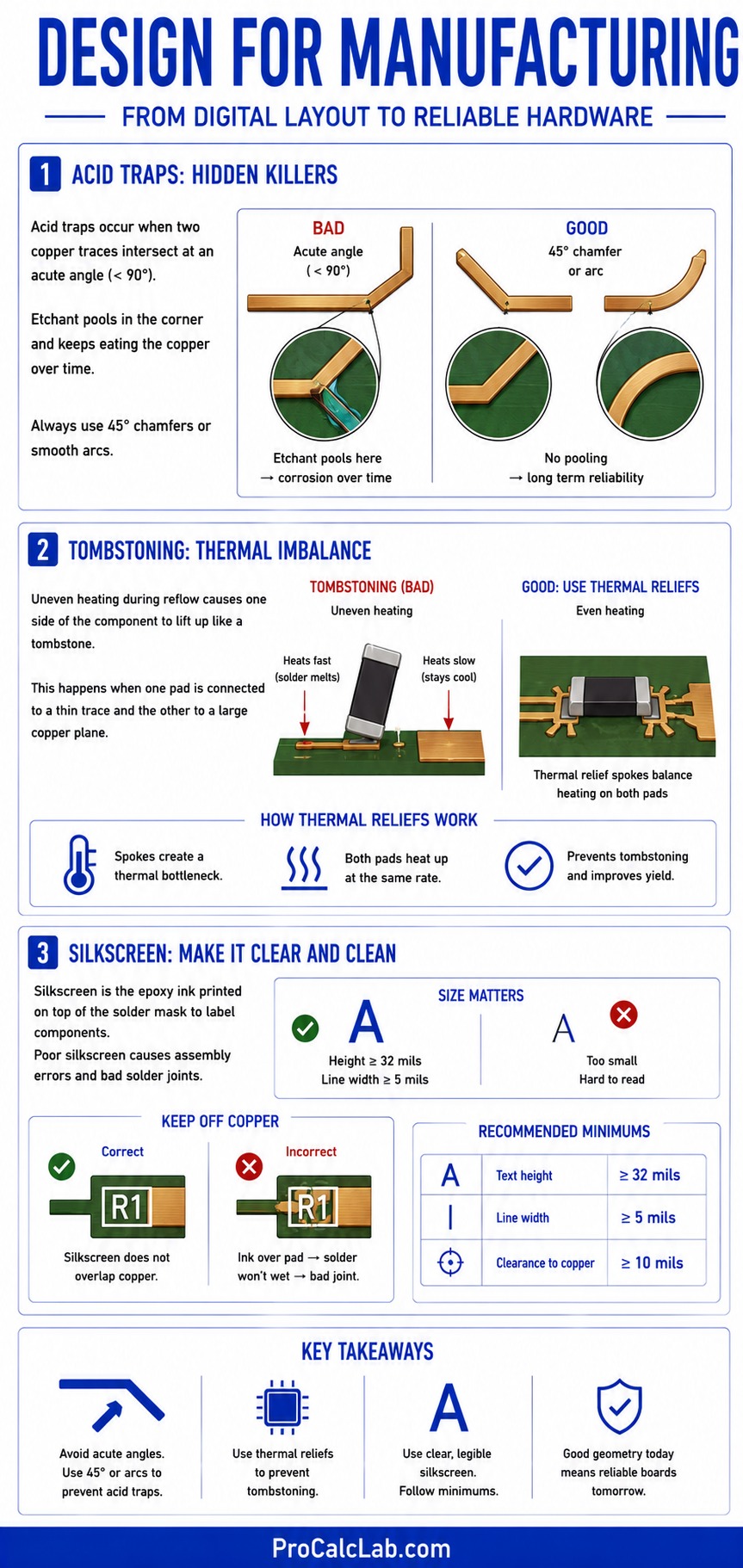
The most common defect we see from amateur layouts is the acid trap. An acid trap occurs when 2 copper traces intersect at an acute angle, meaning an angle less than 90 degrees. During the chemical etching process, the surface tension of the corrosive etchant fluid causes it to pool inside this tight corner. Even after the board is removed from the chemical bath and washed, residual etchant remains trapped in the vertex. Over weeks or months, this trapped acid continues to slowly eat away the copper, eventually severing the trace entirely. To prevent this, always route your traces using 45-degree chamfered corners or smooth sweeping arcs. Never allow traces to merge at sharp, acute angles.
Tombstoning is another massive issue tied directly to poor geometric routing. This occurs during the automated reflow soldering process for tiny surface mount components, like 0402 resistors. If 1 pad of the resistor is connected to a thin 10 mil trace, and the other pad is connected directly to a massive copper ground plane, you have created a severe thermal imbalance. The small trace heats up instantly in the oven, melting its solder paste. The large ground plane acts as a heatsink, keeping its solder paste solid for a few seconds longer. The surface tension of the liquid solder on the hot pad actually pulls the tiny component upright like a tombstone, breaking the electrical connection on the cold side.
📈 To eliminate tombstoning, we utilize thermal reliefs. A thermal relief is a specific footprint pattern where a component pad connects to a large copper plane using 4 very thin copper spokes rather than a solid flood of metal. These spokes provide excellent electrical conductivity while creating a deliberate thermal bottleneck, ensuring both pads of the component heat up at the exact same rate during assembly.
Finally, consider the legibility of your silkscreen. The silkscreen is the epoxy ink printed on top of the solder mask to label components. When working in a zoomed-in browser environment, it is easy to place text that looks highly legible on a 4K monitor but turns into an unreadable white smudge in reality. As a strict rule, never use a silkscreen font smaller than 32 mils in height, and ensure the line width of the font stroke is at least 5 mils thick. Furthermore, carefully inspect your layout to ensure no silkscreen text overlaps exposed copper pads. If ink prints over a pad, the solder will not wet to the metal, completely ruining the electrical joint.
The Translation to Production Data
Once you finish routing your rapid prototype, the web utility must export the visual data into a machine-readable format. The industry standard is the GERBER RS-274X format. This is not an image file; it is a highly precise ASCII text file containing 2D vector coordinates.
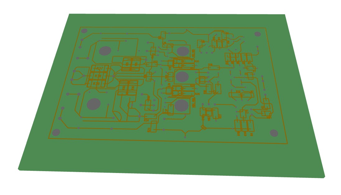
Each physical layer of your board requires a dedicated GERBER file. The top copper, bottom copper, top solder mask, bottom solder mask, silkscreen, and the physical board outline must all be exported independently. Additionally, a separate Excellon drill file is generated to instruct the CNC machines exactly where to plunge the carbide drill bits for vias and through-hole components. A robust browser tool abstracts this complex file generation, allowing you to download a single compressed archive that you can instantly upload to a fabrication house.
Summary
The hardware engineering landscape is evolving rapidly. While massive desktop suites remain necessary for deeply complex, high-speed multi-layer architectures, lightweight web-based tools provide an indispensable workflow for conceptualizing, documenting, and testing rapid prototypes. By strictly controlling UI constraints and offloading rendering physics to the browser, these tools eliminate setup friction entirely. However, designing in a browser does not excuse an engineer from understanding the underlying physics. You must rigorously calculate your required trace widths based on thermal rise, manage your voltage clearances to prevent arcing, and meticulously avoid geometric acid traps. When you merge solid mathematical theory with highly accessible design tools, you accelerate the hardware development cycle exponentially.

Literature
- IPC Standard: IPC-2221 Generic Standard on Printed Board Design. The definitive legal and mechanical baseline for all trace current capacity mathematics and high-voltage dielectric spacing.
- Brooks, D.: Signal Integrity Issues and Printed Circuit Board Design. An essential textbook for understanding the complex physics of voltage drop, characteristic impedance, and thermal management in copper traces.

David Parry — Senior Engineering Analyst
Specializing in electronics and physics-based simulations with 20+ years of engineering experience. David ensures the mathematical and physical accuracy of the tools at ProCalcLab.